This post is a deep dive into the performance and architecture of a gateware block-FFT (Fast Fourier Transform). It is intended for people who really want to understand the circuits in detail with all the nice and nasty details. You should bring some knowledge of complex signals, fixed-point arithmetic and the basic FFT algorithm. An introduction to fixed point math can be found here1, the basic algorithm in python is explained here2 and you might find this3 useful for a background on complex signals.
The FFT is surely one of the most important algorithms in current technology. Since you are probably looking at this on a mobile device, the information in this post went through an FFT circuit (in the WiFi/4G chipsets) at least twice on the way to you.
The core can be configured for arbitrary FFT sizes (in powers of two) and data-widths. It can perform forward and inverse FFT computation onto complex data-samples stored in a block-RAM. After computation, the transformed data-samples can be randomly accessed. An internal computation width of 18 bit maximizes the underlying XILINX/Lattice block-RAM and multiplier architectures and yields >90dB/>80dB/>60dB SNR for 1/8/128 tones if configured correctly. The core can be clocked at >250MHz on an Artix-7 FPGA.
You can temporarily find it here. Eventually the FFT and other DSP cores will be aggregated into a dedicated repo.
Inverse FFT accuracy
Although the core works as FFT or IFFT, the performance is analyzed for a 1024 point, 16 bit (18 bit internal) inverse FFT since the core was originally designed for this use-case.
The ubiquitous FFT algorithm significantly reduces the computational complexity of a DFT by successively applying elementary “butterfly" computations in a divide-and-conquer scheme. The whole FFT is thereby broken up into stages, each of which iterates the butterfly operation over the data. A butterfly computation consists of additions, subtractions and multiplications with “twiddle" factors.
A radix-2, Division In Time (DIT) algorithm shows the best SNR performance of possible fixed-point FFT implementations 4, requires the least resources and is simple to implement. It is, however, also the slowest algorithm. DIT is favorable over Division In Frequency (DIF) since trivial computations are performed first, which leads to better performance. Unfortunately the literature is inconsistent with the DIT and DIF terms. Here DIT will always refer to a division in the input data, agnostic of domain.
The fixed-point arithmetic entails several consequences and particularities in theory of operation. Since the usual inverse Discrete Fourier Transform (DFT)
\[x_n=\frac{1}{N} \sum_{k=0}^{N-1} X_k \cdot e^{\frac{2\pi}{N}jkn},\]where $x_n$ is the n’th time domain sample, $X_k$ the k’th frequency domain sample and $N$ the size of the inverse DFT, features a $\frac{1}{N}$ factor in the computation, a straight-forward fixed-point inverse DFT would occupy only a small fraction of the output dynamic range.
In order to make use of the full output dynamic range we need to scale the computation of the FFT core. Because a single point of scaling would either require the use of a large intermediate fixed-point representation, or introduce significant error, a distributed scaling scheme is employed. Furthermore, a specific shifting schedule can be supplied for each FFT computation so as to maximize the SNR in various scenarios.
This additional control is desirable because we want scaling to happen as early in the computation as possible, so as to not lose precision in the intermediate rounding. This intermediate rounding is inevitable since each input sample is subject to several multiplications during the computation. After each multiplication the output has to be rounded to the internal computation width again. Therefore each rounding operation introduces, on average, 0.25 Least Significant Bit (LSB) of error, if we assume the error to be uniformly distributed. This error is propagated and potentially exacerbated by downstream scaling operations. A more sophisticated error analysis for a fixed-point radix-2 DIT FFT can be found in 5.
An inverse DFT can be seen as a sum of complex sinusoids. Depending on the spectral distribution, the sinusoids can “constructively" accumulate in some time-domain samples or cancel out. For a general vector of frequency coefficients it has to be assumed that the maximum time-domain sample $x_{max}$ will be
\[x_{max}=\frac{1}{N} \sum_{k=0}^{N-1} X_k.\]This has to be considered when choosing a scaling schedule for the FFT core as too much scaling will lead to arithmetic overflows. The scaling schedule should always be optimized so that the output uses the full dynamic range, but not more.
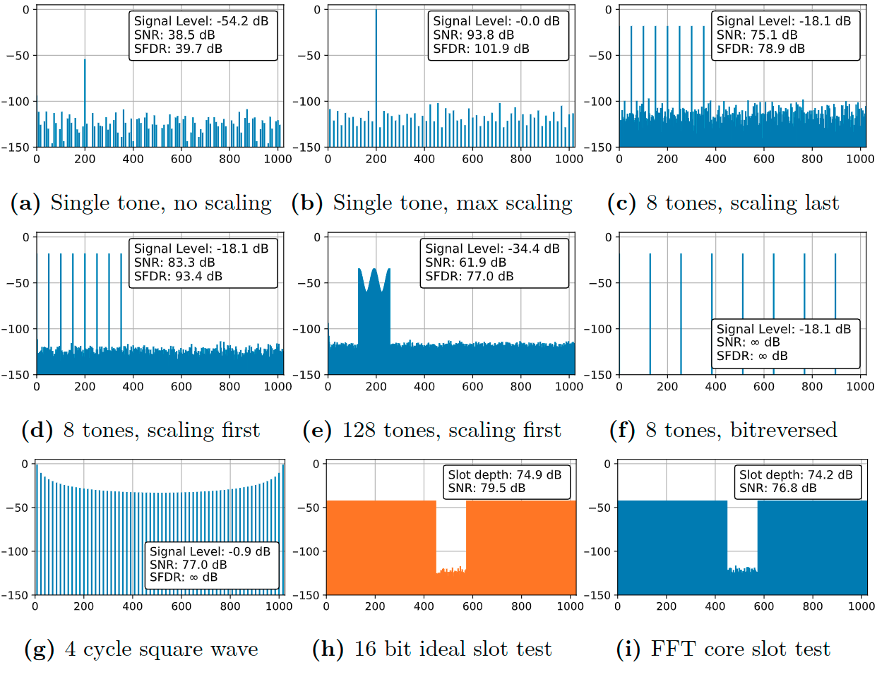
Figure 1 shows the performance of the FFT core for a number of different scenarios. The complex time-domain output of the core is transformed back into the frequency domain by a perfect (double float) FFT and the magnitude of the output is plotted. 1a displays the naive fixed-point FFT performance for a single full-range input coefficient. The noise exhibits some structure as the errors are distributed in the spectrum during the computation. 1b shows an FFT with the same input, but with scaling in every stage. The output tone is now also at full-scale and the noise shows a different pattern. 1c and 1d depict a full-scale output 8-tone FFT with different scaling schedules. 1d shows significantly improved SNR and SFDR, since the early scaling is favorable. 1e portrays an optimized scaling scheme for an arbitrary set of 128 input coefficients. An interesting special case is detailed in 1f, where 8 tones are distributed in a bit-reversed ascending order. Bit-reversing refers to the index written out in binary and then interpreted right- to-left to yield the bit-reversed index. This leads to equidistant tones in natural order, also called a frequency comb. Here the FFT algorithm happens as such that the samples are only shuffled around and never multiplied with non-trivial twiddle factors. The resulting time-domain pulse comb is perfectly expressed in fixed-point representation.
 |
|---|
| (1) 9 IFFT computation scenarios for the developed core. |
Another interesting case is demonstrated in 1g. The scaling scheme allows for the synthesis of a full-scale time-domain squarewave, even though two full-scale tones at arbitrary positions would lead to overflow. 1h and 1i show the output of a “slot test”. For a slot test all of the FFT frequency bins are initialized with maximum amplitude, random phase samples. Then a “slot” is cut out by setting a number of consecutive samples to zero. Afterwards the FFT of the remaining “depth” of the slot is compared. 1h has been computed with an “ideal” double precision float FFT and then time-domain quantized to 16 bit. 1i shows that the output of the FFT core has comparable performance.
The SNR is calculated as follows: Signal power is defined as the ideal signal power output by an ideal FFT (with the same scaling as the core). The error signal is determined by subtracting the ideal signal from the FFT core output. The noise power is defined to be the power of this error signal, with the SNR being the ratio of the two terms. Note that this is a stricter SNR than the usual SNR calculation, where signal and noise bins are defined in an output spectrum.
Architecture
 |
|---|
| (2) FFT Block-Diagram. |
In a block-FFT the data is always stored in the same location and iterated over to compute the FFT. At the end of computation, the data is transformed into time-domain and samples can be randomly accessed. The overall block diagram is depicted in Figure 2 with the individual blocks explained later in the text.
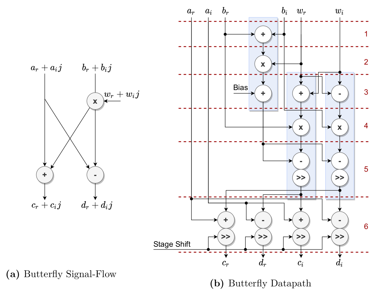
As we want the computation to happen as fast as possible with reasonable resource overhead, the design features a single, fully pipelined butterfly computation core. This core ingests two input samples $a,b$ and one twiddle factor $w$ and expels two output samples $c,d$ in each clock-cycle. Separating the computation of the output samples
\[c=a+wb\] \[d=-a+wb\]into their real/imaginary components
\[c_r=a_r+b_rw_r-b_iw_i\] \[c_i=a_i+b_rw_i+b_iw_r\] \[d_r=-a_r+b_rw_r-b_iw_i\] \[d_i=-a_r+b_rw_i+b_iw_r\]and then rewriting the complex outputs as
\[c_i=a_i+(b_r+b_i)(w_r+w_i)-b_rw_r-b_iw_i\] \[d_i=-a_r+(b_r+b_i)(w_r+w_i)-b_rw_r-b_iw_i\]yields a set of equations with 3 real multiplications in total. Note that the same multiplication is present in several equations and therefore only requires a single instatiation in the circuit.
Allocating the equations to arithmetic primitives in the FPGA yields the datapath shown in Figure 3. The full computation can be accomplished using only 3 DSP blocks and 4 fabric adders. To achieve a high fabric clock, a pipeline register is located after every elementary arithmetic operation. The core thereby uses 6 computational steps plus one step at the input and output to pipeline the memory access. There are shifting operations in two of the computational steps. The second shift is configurable by an additional shift input and actualizes the stage scaling. When there is no scaling, the output is shifted by one, hence applying a factor of $\frac{1}{2}$. Doing this in every stage leads to the “natural" $\frac{1}{N}$ factor in the inverse DFT computation. If the output should be scaled in the current stage, the output is not shifted which can lead to bit growth on the output.
 |
|---|
| (3) Butterfly Signal-Flow and Datapath. The blue boxes signify the underlying DSP block actualization. The dashed lines signify pipeline register stages. |
The first shifting operation, at the output of two DSPs, is used in conjunction with the bias to implement rounding. The rounding makes use of the fact that multiplication output width is the sum of the widths of the inputs. By adding a constant equivalent to 0.5 input LSBs to the output, where one input LSB is represented by many bits, the output gains this offset. After shifting behind the output, the offset is negated by the negative offset introduced by the shifting operation. This procedure actualizes the “round half up" rounding scheme.
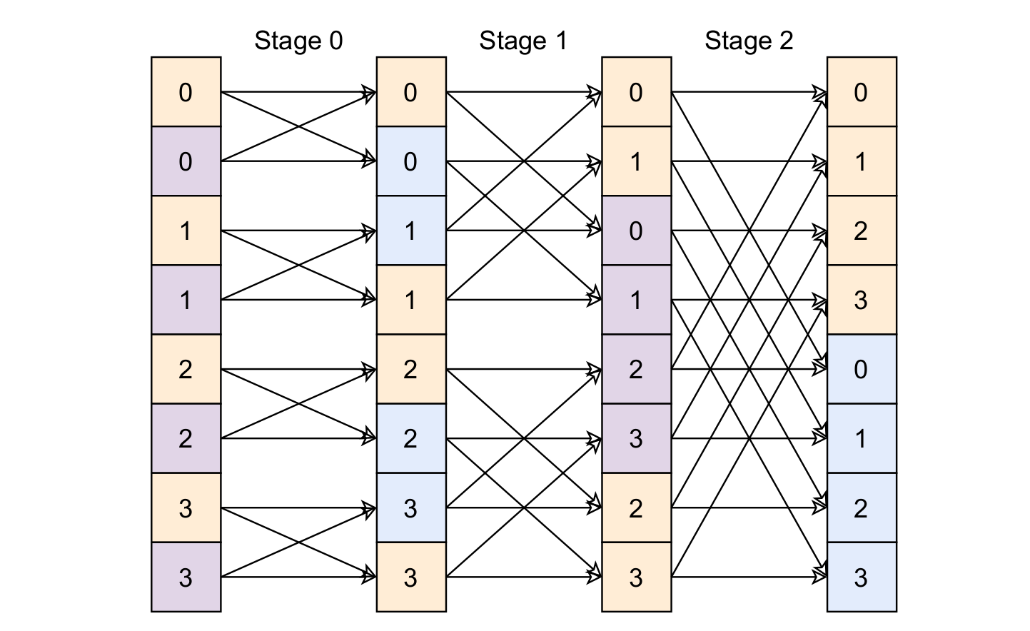
The butterfly computation iterates over the data vector once per FFT stage. Since the data is stored in a RAM block in the FPGA, the correct addresses of the inputs and outputs must be computed. Because we want a total of four memory locations to be accessed in one cycle, we need at least two dual-port memories. However, because the order of access changes in every stage, we need a predictive scheme which sorts the outputs of the butterfly core into memory in a way that allows a future butterfly operation to access inputs from different memories.
The matter is further complicated by the fact that the butterfly core has an 8 cycle pipeline delay. This delay leads to memory access congestion at the stage transitions, where input data from the new stage is accessed, but the output data is 8 cycles delayed and therefore still from the last stage. To remedy this problem, the FFT core alternates two separate memories for the second butterfly input and output. There are better schemes which do not require for an extra memory bank by additionally accounting for the pipeline delay and altering the computation order within a stage 6. The memory access pattern is illustrated in Figure 4.
 |
|---|
| (4) Simplified 8 point FFT memory banking scheme. The memorybanks are illustrated with different colors and the respective entry address is shown. RAM1 is shown in orange, RAM2a in purple and RAM2b in blue. Using this scheme, neither the butterfly inputs nor the outputs ever access the same memory bank. |
The memory logistics as well as the FFT input and output access are aggregated into the data scheduler circuitry. This module also keeps track of the computation flow and sets the butterfly scaling signal in the relevant FFT stages. The scaling schedule is simply a register in the data scheduler accessible from outside. The scheduler has the additional task of allocating the FFT input data to the memories and bit-reversing the addresses, if configured to do so. The bit-reversing is an integral part of the FFT algorithm. At the output, the scheduler acts as an address decoder, abstracting the multi-memory architecture for downstream modules.
Using an internal data width of 18 bit, one complex sample maximizes the 36 bit architecture of the XILINX RAMB36 primitives. Therefore the real and imaginary parts also maximize one input of the DSP48E1 18x25 multipliers. The data memories fully occupy the 9 bit address space of a RAMB36 block for a 1024 point FFT. The same datastructure is used for the twiddle factors, hence occupying a single RAMB36 block. Additionally the twiddle factors are compressed, exploiting the symmetry of the unit circle. The mapper uses the leading three bits of the twiddle address to rotate the twiddle factors stored at the address defined be the remaining bits to the correct eighth of the circle.
There is a nice synergy between the 16 bit input data, the 18 bit internal precision and the radix-2 DIT scheme. In this FFT variant, all of the twiddle factors in the first two stages point in the direction of the real or imaginary axis and are therefore perfectly represented in fixed-point arithmetic. In conjunction with the fact that we can always scale the first two stages because we can let the inputs grow to 18 bit, we avoid rounding errors in the first two stages. As stated before, errors in the beginning of the computation are the most critical.