This posts presents the development of a variable rate-change, super-sampled, high performance interpolator core. The discussed techniques require some knowledge of digital signal processing, specifically Half-Band Filters (HBFs) and Cascaded Integrator Comb (CIC) filters. This1 article gives a good introduction to CIC filters. Tomverbeure’s blog is a great read on HBF filtes2 and a decimator cascade3 that inspired some of the plots here. Armed with this knowledge you might find a few advanced architectural tricks in this post that I found to be hard to come by just searching the internet.
Interpolators are necessary in any Direct Upconversion (DUC) scheme where a slow baseband signal is upconverted by a fast digital carrier. With modern gigasample dataconverters it becomes increasingly difficult to build fast circuits that run at the full sample rate. Hence a super-sampled architecture is often necessary, computing multiple output samples in one clock cycle.
The core presented here operates 2x super-sampled and can be dynamically configured to various rate changes. It internally uses 18 bit signals since this maximizes the dsp-block resources and achieves an alias rejection of greater than 89.7dB for all interpolation rates. The interpolator features a finite impulse response and the maximum rate-change configured at synthesis can be very high (>8000 tested). In this configuration the full interpolator has an impulse response of several 100000 samples and thus performs a lot of raw compute. The background picture on top shows a small part of the impulse response for a rate-change of ~50. The core can be clocked at >250MHz on an Artix-7 FPGA.
You can temporarily find it here. Eventually the interpolator and other DSP cores will be aggregated into a dedicated repo.
Performance
Finite Impulse Response (FIR) Half-Band Filters (HBFs) are efficient linear phase filters. By imposing the constraint \begin{equation}\label{1} H(e^{j\Omega}) + H(e^{j\Omega-\pi}) = 1, \end{equation} where $H$ is the frequency response and $\Omega$ represents the normalized angular frequency in radians per sample, and \begin{equation} N=(4\cdot n)-1, \end{equation} where $N$ is the number of filter taps and $n$ is a natural number, the frequency response is centered around $\Omega/2$. As a result, every second coefficient, except for the center tap becomes zero. Additionally, the symmetrical impulse response halves the number of multiplications and makes use of DSP pre-adders. A polyphase decomposition of a $R=2$ HBF interpolator leads to the aggregation of the non-zero multiplications in one polyphase path. The other polyphase part reduces to a unity-gain delay4.
A Cascaded Integrator Comb (CIC) filter is a special case of a multiplier-less FIR filter. As the name suggests, instead of delaying and multiplying the input, it constitutes a cascade of integrator and comb stages. While this arrangement makes for a very resource efficient implementation, the filter has a limited range of possible frequency responses. However, as no new filter coefficients have to be provided, the response can be adapted easily during operation.
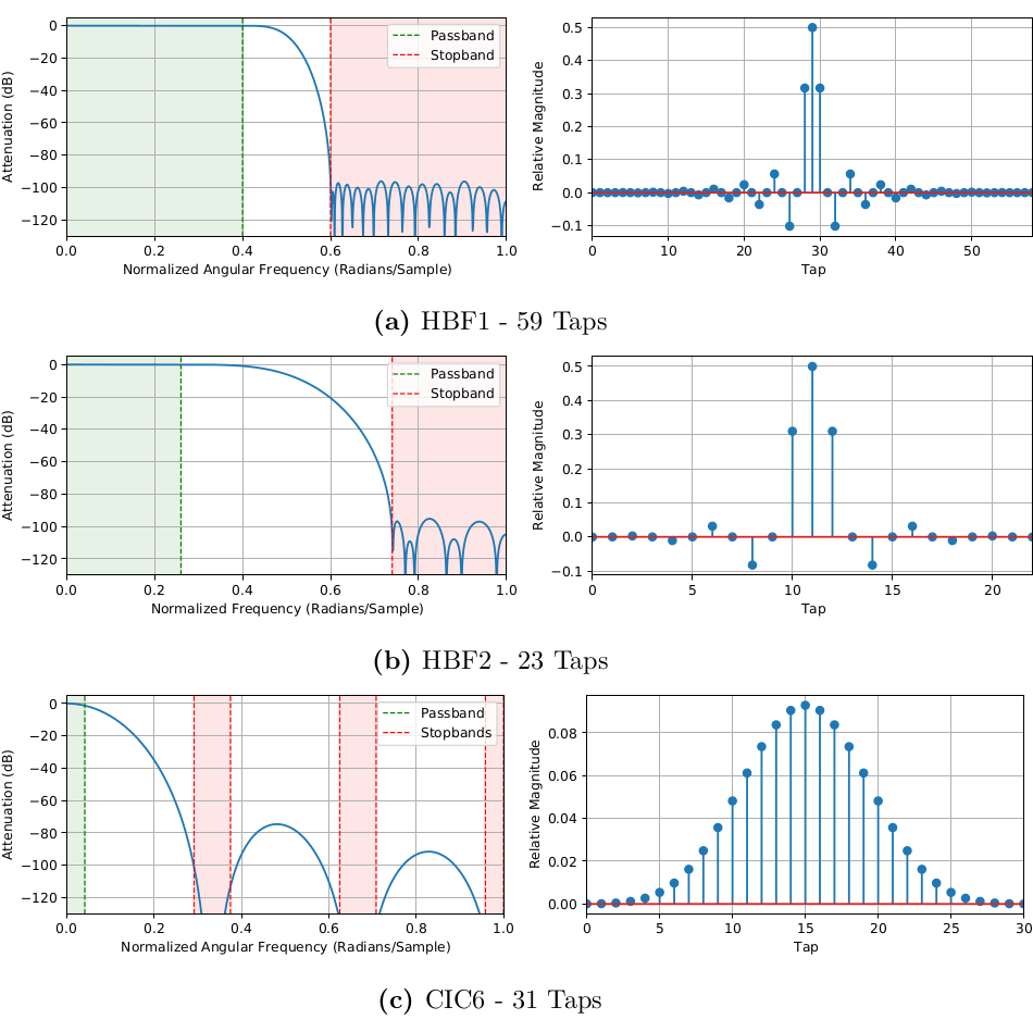
Since a monolithic filter for the whole interpolator would not be very flexible or efficient, a variable filter cascade is employed. At $R=2$ the interpolator uses a single, sharp HBF with a transition band form $\omega_p=0.4\Omega$ to $\omega_s=0.6\Omega$, with $\omega_p$ being the passband frequency and $\omega_s$ the stopband frequency. The minimum HBF size for an image rejection of higher than 90dB is 59 taps using the Parks–McClellan/Remez algorithm. Due to the high stopband attenuation and the symmetrical nature of the frequency response, passband ripple is not a concern. A zero stuffer inserts a zero between each sample and the filter input (in the actual implementation this zero stuffer is abstracted away, see architecture). The frequency magnitude and impulse response is shown in Figure 1(a).
 |
|---|
| (1) Frequency magnitude and impulse response for the three interpolator filters. |
The $R=4$ interpolator uses the $R=2$ interpolator described above with a second $R=2$ stage. The second stage has the same structure as the first. However, the design constraints for the second HBF are relaxed in comparison to the first. Since the first stage already suppresses images above $\frac{1}{2}\Omega_1$, with $\Omega_1$ being the normalized angular frequency of the first HBF, there can also be no significant aliases between $\frac{1}{4}\Omega_2$ and $\frac{3}{4} \Omega_2$, with $\Omega_2$ being the normalized angular frequency of the second HBF. As displayed in Figure 1(b), a HBF with 23 taps is sufficient for an image rejection of >90dB in the stopband.
For interpolation rates greater than four, the interpolator constitutes the two HBF stages and a third CIC stage. Because the second HBF stage has halved the passband again, the design constraints are further relaxed. As the CIC frequency magnitude response \begin{equation} |H(e^{j\Omega})| = \displaystyle\left\lvert \frac{sin(\Omega D/2)}{sin(\Omega/2)}\right\rvert^M, \end{equation} where $M$ and $D$ are the CIC order and differential delay of the comb stages, has troughs around \begin{equation} T_n = \frac{n}{D}, \end{equation} with $n$ being a natural number, we prefer the passband to alias into those troughs. This is given when \begin{equation} R_{CIC}=D. \end{equation} An example for $R_{CIC}=6$ is depicted in Figure 1(c).
 |
|---|
| (2) Composite frequency responses for various interpolator configu- |
| rations. |
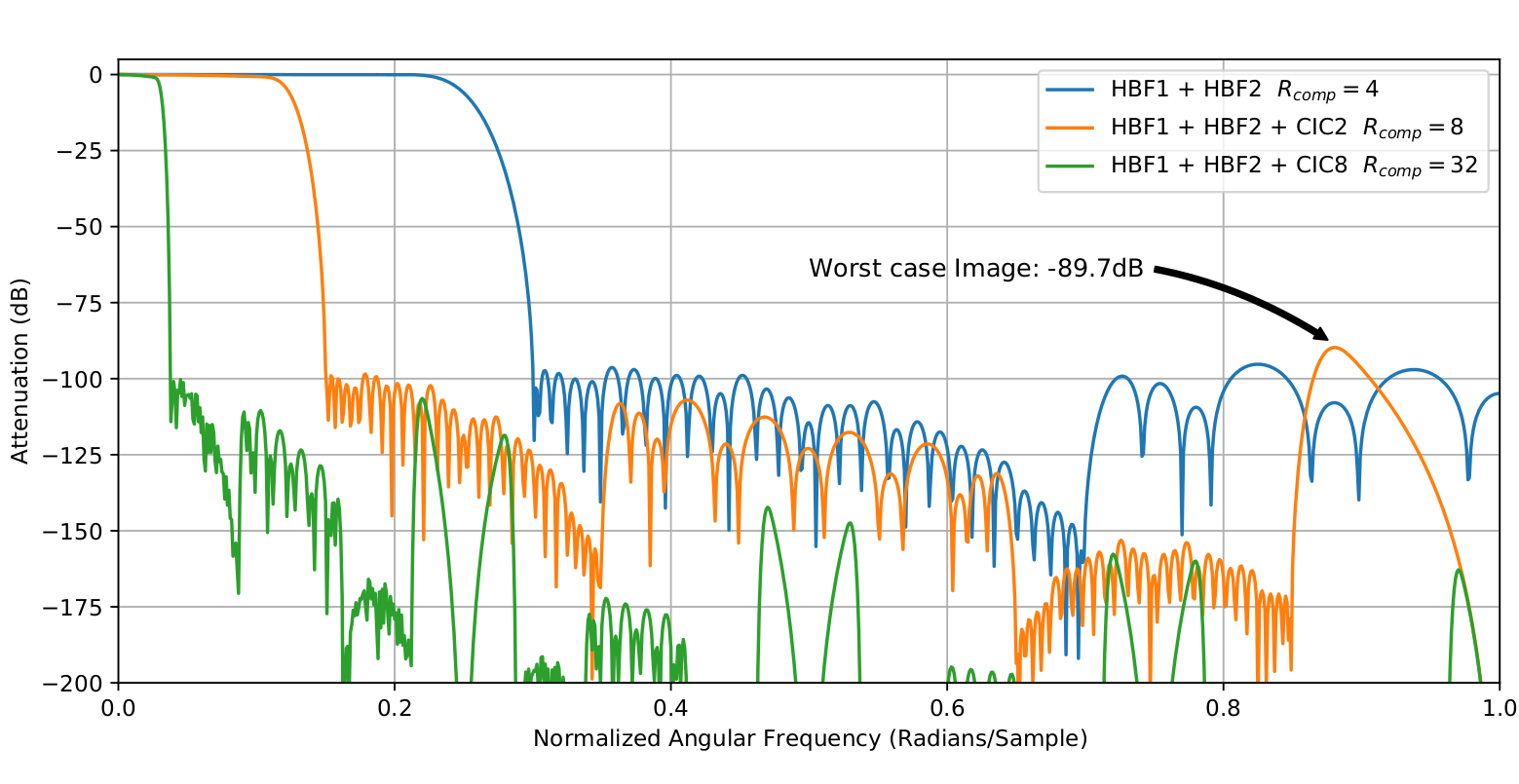
As we need the CIC stage to realize rate-changes of 2 to 1024, the CIC has to provide >90dB image rejection for all configurations. It was found that a 6th order $M=6$ CIC at $R=D=2$ is just barely short of this performance. Nonetheless, 89.7dB of image rejection was deemed sufficient. As shown in Figure 2, the aliases are attenuated further at higher rate changes.
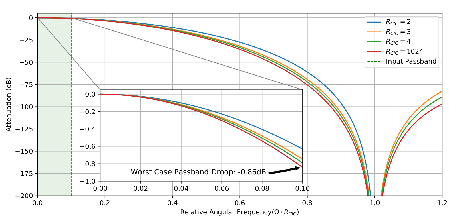
Unfortunately, a CIC filter exhibits inevitable drooping of the passband. This droop is exacerbated as the rate-change and thus differential comb delay increases. For the interpolator, this is effect is mitigated by the fact that the passband is compressed by the two leading HBF stages. The droop for a selection of rate-changes is plotted in Figure 3. For this interpolator a worst-case of -0.86dB was deemed tolerable. A small, even multiplier-less, compensation filter could be added in the future.
Another downside of the cascaded interpolator architecture is that the rate change can not take any value. $R_{CIC}$ can be any natural number greater than 1. However, as the composite rate-change is multiplicative \begin{equation} R_{comp}=R_{HBF1}\cdot R_{HBF2}\cdot R_{CIC}, \end{equation} this entails a rate-change granularity of 4 for the whole interpolator at $R>2$.
 |
|---|
| (3) CIC passband droop for various rate-changes. |
Architecture
As the interpolator must be synthesized with the necessary performance (performance in the architectural context refers to the maximum clock rate for the gateware), further optimizations in the implementation are necessary. Though the first stages often run at a sample rate $R$ much slower than the FPGA fabric clock $R_{CLK}=250$MHz, every stage can potentially be the last and therefore have to serve the DAC at $R_{DAC}=500$MHz. Consequently, a 2x super-sampled architecture is necessary for every filter. Super-sampled refers to the fact that the circuit processes more than one sample per clock-cycle.
For the HBFs, we can exploit the multirate decomposition for supersampling. Since every second output sample is just a delayed version of the input and the other polyphase path runs at the input sample rate, we can run them both at $R_{CLK}$ to achieve a throughput of $2R_{CLK}$. The nontrivial path is fed with one input sample per cycle and no stuffed zeros, leading to a standard filter.
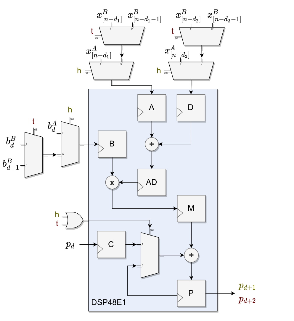
To stay within the 240 DSP limit of the FPGA, a custom, DSP multiplexed architecture with several optimizations is employed for the HBFs. First it is realized, that the number of operations per cycle stays roughly constant whether just HBF1 or HBF1 and HBF2 are engaged. This is because HBF2 is approximately half the size of HBF1 and HBF1 always operates at $R_{HBF1}=R_{HBF2}/2$. Hence, it is possible to time-multiplex the resources of HBF1 when HBF2 is engaged, freeing up the rest of the DSP blocks for HBF2 computation.
This results in the multiplexed DSP architecture illustrated in Figure 4. The XILINX DSP48E1 DSP circuitry (see XILINX DSP Usage Guide5 for details) is shown in blue with all of the internal registers and arithmetic enabled. The $d$ delayed filter inputs $x_{[n-d]}^A$ for filter A and $x_{[n-d]}^B$ for filter B are multiplexed into the pre-adder inputs, while the $b_d^A$ (filter A) and $b_d^B$ (filter B) filter coefficients are multiplexed into the multiplier input. When the multiplexing signal h is true, the DSP computes one output of one filter tap \begin{equation} p_{d+1}=((x_{[n-d_1]}^A+x_{[n-d_2]}^A)\cdot b_d^A ) + p_d \end{equation} in one clock-cycle for filter A. When h is false, the t signal alternates between true and false with a two cycle period. This leads to the computation of one accumulated output of two filter taps \begin{equation} p_{d+2}=((x_{[n-d_1]}^B+x_{[n-d_2]}^B)\cdot b_d^B ) + ((x_{[n-d_1-1]}^B+x_{[n-d_2-1]}^B)\cdot b_{d+1}^B ) + p_d \end{equation} every second cycle.
 |
|---|
| (4) Signal flow of the multipexed DSP architecture. |
With all of the optimizations, HBF1 requires 15 multiplications to compute two new output samples and HBF2 requires 7. Therefore, the whole DSP cascade consists of 15 multiplexed DSP blocks. When only HBF1 is engaged, h is true and filter A takes the role of HBF1 for all DSPs. If both HBF1 and HBF2 are engaged, h is false for the first 8 DSPs and filter B now becomes HBF1. In the latter 7 DSPs h is still true with filter A now actualizing HBF2.
There are a few additional adjustments necessary to make the architecture execute the desired function. First, the trivial polyphase sample from HBF1 has to be piped into the input of HBF2 with the correct delay. Second, a zero multiplication has to be injected in the last time-multiplexed DSP because HBF1 requires an odd amount of multiplications. Third, as filter rounding for the DSPs is performed by piping an offset value into the C input of the first DSP block, this offset must be applied every second cycle for filter B.
Using this arrangement, the second HBF can be implemented at zero DSP cost. The downside is that the multiplexers use more fabric logic, though this was not the limiting resource.
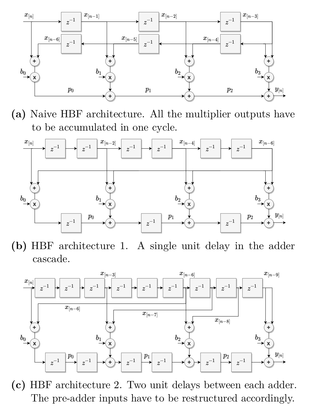
In order to make the interpolator meet the $R_{CLK}=250$MHz timing requirements, pipelining has to be used between each arthmetic operation and DSP block. During development it was found that the C register of the DSPs was not necessary to meet timing in a design containing only one interpolator. Yet, with several interpolators in a big design, it was found that the C register is required. As the C register actualizes a unit delay between the postadders in the DSP chain, the filter topology had to be adapted. Figure 5 shows three iterations of HBF topologies with the last one being utilized in the final interpolator.
 |
|---|
| (5) Three iterations of the HBF topology. |
For most interpolation rates the CIC stage is last and hence it is required that the CIC operates super-sampled as well. Since we use the CIC for interpolation, only the integrator stages have to run at the output sample rate and thus super-sampled. This is accomplished by operating two separate interpolators in each stage, one of which accumulates two input samples per cycle. Both integrator outputs are passed onto the next stage where the first integrator accumulates the first input and the second integrator accumulates both. Aside from the accumulator register there is one more pipeline register in each stage for pre-adding the two inputs.
Another consequence of the super-sampled CIC scheme is that the interpolator stage does not ingest samples at evenly spaced intervals for uneven interpolation rates. For $R_{CIC}=3$ the core ingests on average ~0.66 samples per cycle and expels exactly two. In other words, the stage needs to wait on average ~0.33 cycles between every input sample. To account for this, the stage alternates the waiting periods between the closest natural numbers so that the average rate is correct. As a consequence, all of the differentiators have to be run at this staggered clock. Furthermore, additional logic is necessary to ensure the correct output stalling behavior in the upstream HBFs.
Owing to the high $M=6$ filter order, the integrator accumulator widths become very large for the latter stages. Since the register bit width is given by \begin{equation} W_{reg} = W_{in} + ((M-1) \cdot log_2(R)) \end{equation} with $W_{in}$ being the input bit width, it follows that \begin{equation} W_{reg} = 66 \textrm{bit} \end{equation} for a maximum rate-change of 1024 with 16-bit inputs. Fortunately, thanks to fast carry logic in the FPGA slices, a 66 bit adder is realizable at $R_{CLK}=250$MHz.
Also, since \begin{equation} |H(0)| = R^{M-1}, \end{equation} the DC gain of the filter becomes very substantial and not a power of two in many cases. It can thus not be compensated via simple bitshifting. To overcome this problem the CIC uses a Look-Up Table (LUT) with compensation values in a custom format. There are 11 bit of linear, fractional, fixed-point gain which is applied at the input of the CIC and 7 bit of bitshifting (i.e. power of two) gain, which is applied at the output. This compromise uses just a single DSP at the input, one RAMB18 block and some logic for the variable bitshifting at the output. The DC gain is essentially unity using this scheme.
An approach to build a multiplier-free interpolator would be to employ a “Sum Of Powers Of Two” (SOPOT) architecture similar to6. Here the hardware multipliers are replaced with clever bitshifting and addition to make for very efficient, though not very flexible, filter tap computation. The restricted choice of filter coefficients could lead to a minimal increase in filter size, as the zeros of the transfer function do not land exactly on the unit circle.
References
-
A Beginner’s Guide To Cascaded Integrator-Comb (CIC) Filters ↩
-
Heinz G Göckler. “Most efficient digital filter structures: The potential of halfband filters in digital signal processing.” ↩
-
SC Chan and KS Yeung. “On the design and multiplier-less realization of digital IF for software radio receivers with prescribed output accuracy.” ↩